HTML5 compliant


Design Approach
I have obtained various kind of experience in
semiconductor industry in both Japan and US. The excerpt of my resume
below exhibits the broad experience.
SUMMARY
Creative professional with broad technical knowledge and over 16 years of VLSI
engineering experience in both Japan and USA which includes managing
and designing a wide range of foremost VLSIs, graphics, MPEG, USB, flash memory.
Background encompasses from front-end to back-end entire VLSI development
phases such as product planning, architectural design, logic design, circuit
design, mask-layout physical design, bread-board/evaluation system design,
embedded software design, LSI test, and others.
Author, lecturer, and holder of 13 US patents. Excellent analytical skills for
resolving complex problems. Action
oriented leadership with innovative ideas for strategic product development.
Continuously pursuing advanced technologies.
When we develop VLSI, utilizing FPGA is inevitable to verify the functionality
under actual system. FPGA nowadays provides us sufficient speed and amount
of gates. Accordingly, we can easily make any kind of VLSIs done the
functional verification by FPGA combining the Verilog/VHDL simulator and logic
synthesizer in both Unix and PC platform.
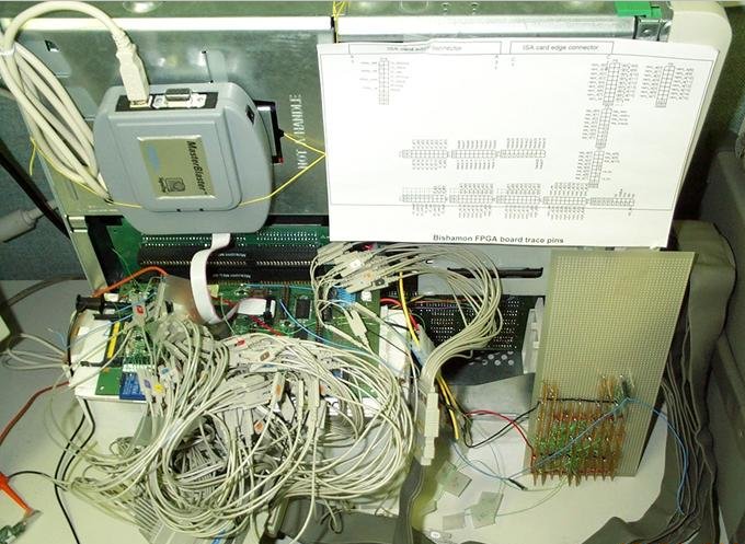
Long time ago, we had to make a bread board using TTLs and PALs every time we
develop a certain LSIs. The last time we made the bread board was
for the development of µPD72120, advanced graphics display processor, in NEC over 15 years ago. It needed
12 24"x24" PCB boards mounted on vertical rotatable book shelf and amazingly
worked by making every one of possible efforts although the operating frequency
was under 2MHz. As a result, I was able to make graphics BIOS and visit
customers showing the demonstration system before working silicon was made
later.
FPGAs have surprisingly advanced today. Additional feature of automatic
test vector generation will be provided soon and the effort to make the test
vector will be unnecessary. Software people who do not know how the gates
are made with the knowledge of device physics, how the test vector should be
made, and how the VLSI must be tested out thoroughly, can design actual physical
VLSI products that are shippable as they design software. The age of
silicon software has come.
However, only a person who actually experienced broad category of the
development work can handle all things efficiently and effectively in the real
world, not in imaginary optimistic world as mass media people are drawing and
most people are dreaming. The person must know everything about hardware
and software, device and system, engineering and marketing.
The most important factor is intuition derived from such over-all experience.
The person can instantaneously discriminate the truth and the false (Honmono
to Nisemono).
I presented Bishamon (USB to CF/MMC/SD flash memory Bridge LSI) at Santa Clara Convention Center in October,
2000 discussing about USB flash memory and predicted the future replacement of
floppy disk drive by USB flash memory stick at the end.
High resolution slides
A couple of small examples attached exhibits how I proceed to study and develop
things practically. It is not necessary to say that the design approach
exhibited here can be applied to very large scale development as well.
The PDF documents below contain block diagrams, timing charts, emulation C
source code, Verilog HDL source code, and the Verilog simulation result
exhibiting the wave form.
(1) NRZI (Non-Return-To-Zero) encoder & decoder
(2) CRC16 (Cyclic Redundancy Check: X16+X15+X2+X0) generator
(3) CRC5 (Cyclic Redundancy Check: X5+X2+X0) generator
(4) USB SIE (Universal Serial Bus Serial Interface Engine) receiver

